1、第一步,打开PCB editor设计软件;

2、第二步,设置语法:PROPAGATION_DELAY=A:B:C:D
A:起点pin
B:终点pin
如果整条线NET只有两个pin时,在A处写入L,B处写入S;
C:最小线长
D:最大线长
例如:PROPAGATION_DELAY=U1.10:U2.10:1000mil:1500mil,设定U1.10到U2.10的走线长度为1000mil到1500mil之间;PROPAGATION_DELAY=L:S:1000mil:1500mil,设定整条NET走线长度为1000mil到1500mil之间;
点击edit-properties;
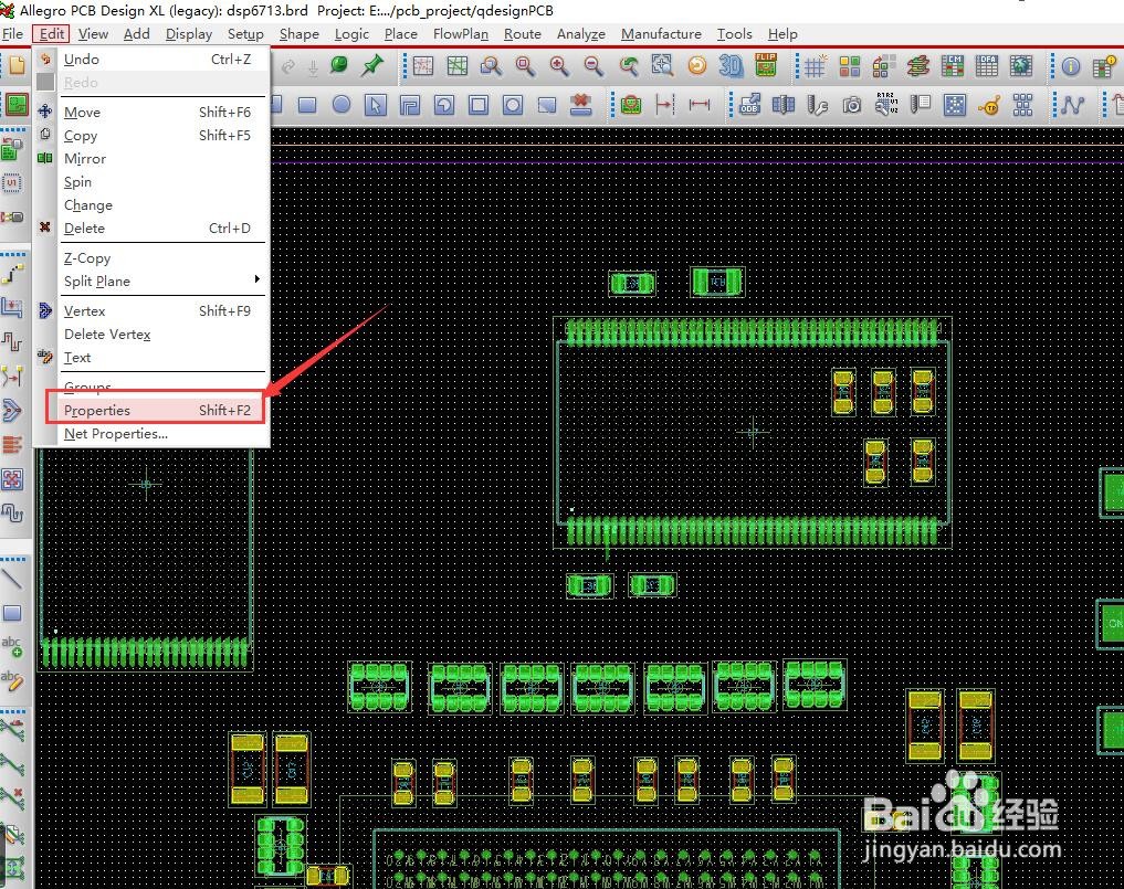
3、第三步,执行edit/properties后,选择一个网络;
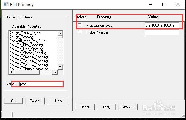
4、第四步,在左侧搜索框中输入“pro*”,找到PROPAGATION_DELAY,然后键入有限值,点击apply;
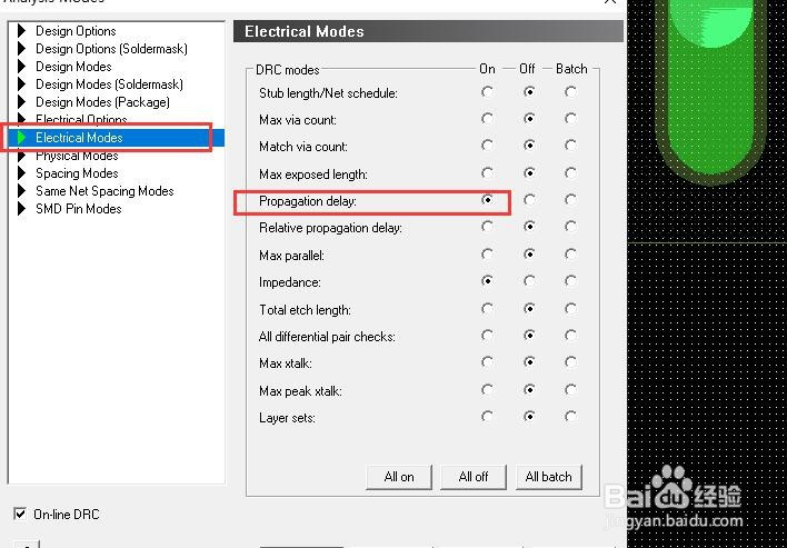
5、第五步,开启检查模式,setup-constraint-mode,找到electrical modes--propagation delay,打开开关即可;
1、1-打开PCB editor设计软件;
2-点击edit-properties,
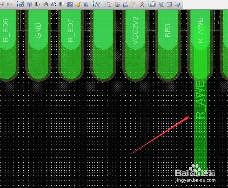
3-执行edit/properties,选择一个网络,比如R_AWE;
4-在左侧搜索框中输入pro*,找到PROPAGATION_DELAY,然后键入有限值,点击apply;
5-然后开启检查模式,setup-constraint-mode,左侧选择electrical modes,右侧打开propagation delay的开关;